| Voltage Controlled Delay with the PT239x |
This page discusses the PT239x series delay chips made by Princeton Technologies. Here I will post notes about my experiences with these ICs as well as complete designs for delay circuits. All of the PT chips used in these projects can be purchased at small bear electronics
PT2395 Echo
PT2396 Short Delay Effects
PT2399 Delay - updated
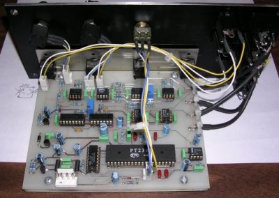
| PT2395 Echo: PT2395 data sheet This is a voltage controlled echo module. It is based around the Princeton Technology PT2395 delay IC. The main features are:
|
 |
This circuit can not reach delays short enough for chorus or flanging. The shortest delay possible is some tens of milliseconds. I cannot remember exactly how long it was but, I can say that at minimum delay time, with no feedback, the echo is still barely audible. The maximum delay is about 1.5 seconds in 256Kb mode. Since I first posted this design, I have received several emails asking about a printed circuit board for the project. I have been considering an updated version but now it is looking like I will make a more advanced dual PT2399 delay (see below). If that idea falls through, then I'll be back to make a new PT2395 delay. For now check out the original version:
Version 1 Documents:
| vc-echo-schem_03-05-2005.pdf - schematic diagram. If you have an old version make sure that R19 should be 270K-300K instead of 100K. I noticed reccently that my 78L05 regulator was running a little hot. A 7805 would probably be a better choice. |
| vc-echo-doc_03-05-2005.pdf - Circuit description and calibration procedure. |
| vc-echo-panel.fpd - This is a front panel express design file that matches the Oakley Sound panel format.. |
I have recorded some sounds to give an idea of what the module is capable of. Every time I go to record something I get side tracked just playing with it, but here is what I have:
Sounds:
| sequence - random arpeggiator sequence. the CV inputs were not connected yet when I recorded this. towards the end I'm slowly adjusting the delay time pot. |
| modulation - just a slight amount of modulation from a slow traingle VCO. An oakley equinoxe phaser is in the feedback path which is also modulated by an LFO. |
| echo-verb2 - a slightly more complicated patch. 2 VCOs, 1 lowpass VCF, 1 VC-Echo, 1 ADSR, 1 LFO and a TLN-156 reverb. a slow moving LFO modulates the trauma setting on the the TLN-156, the filter cutoff and also triggers a very slow ADSR. the ADSR modulates the delay time. stereo left and right are recorded twice. both are the same patch but the LFO phase is different on each channel. |
| QRVG echo - This one used a quantized random voltage generator module I was working on. That module is not finished due to a bug in either hardware or software (not sure yet), but this example shows the echo more clearly than the previous examples. It may get a little boring; it wasn't meant to be a demo of the delay actually. |
| theremin echo - as the title suggests. I was running a theremin through the delay. The theremin was not finished at this time (I decided to redesign, and I haven't finished it yet). Only the pitch antenna is connected during this test. |
PT2396 Short Delay Effects (planning): PT2396 data sheet
The PT2395 is a good chip for echoes, but I am also interested in chorus and flanger effects using a few very short delay lines. In preperation for this project, I am going to be experimenting with the PT2396 IC. The PT2396, has an internal RAM but still requires the external clock. Some information in the data sheet leads me to believe that the RAM has multiple taps. Using a 4-bit digital input, the delay time can be set between 12msec and 200msec. In addition to the digital input, the external clock can be a VCO. I have ordered several PT2396 chips to experiment with. For this project to work, I will need to be able to clock the chip over a wide range. The data sheet specifies a 2MHz clock, but does not specify minimum or maximum clock rates. I am hoping that the PT2396 allows clock frequencies similar to that of the PT2395. This may not work at all. If that is the case, I will probably just use some BBDs. More info later.
PT2399 Notes: PT2399 data sheet
The PT2399 is PTC's latest delay IC. It is also the easiest to work with. This is a single chip delay with a built in VCO and 44Kb RAM. It can produce a deccent range of short echoes. I would have used this for my original VC-Echo but, unlike the PT2395, its RAM cannot be increased. The example circuit in the PT2399 data sheet will work ok except I wasn't happy with the distortion at longer delay settings. I have decided to try and build a new delay using the PT2399. Having most of the circuit on a single chip is nice, and Princeton Technologies told me in an email that this one is superior to the others. This seems to be their only chip that was not a replacement for some other delay IC.
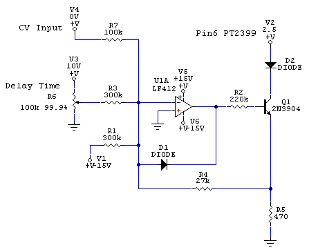
The delay time is set by a resistor connected to pin 6 (VCO pin). The voltage at pin 6 stays at 2.5V so the adjustable resistor is aparently setting the current for the VCO. I know of three ways to add voltage control to the PT2399. The method that I have used is an NPN current sink attached to pin6 of the PT2399. Scott Bernardi used a current source controlling a Vactrol to adjust the resistance. Scott Stites has also informed me that a FET voltage controlled resistor works well. If one is not careful, a PT2399 can be destroyed with the current sink. I am not totally sure how, but I have done this on the breadboard. I was quite a beginner at that time anyway. It wasn't until reccently that I purchased some new PT2399s. I have tested a new circuit that has min and max current limits (0mA to 3mA).

The current through R1 sets an initial current (2.9mA measured). Any CV added reduces the output current. I haven't tested what minimum current is needed, but when I find that out, I will probably add a resistor from the PT2399's pin6 to ground. The opamp I am using is actually a TL072. The maximum current does not occur exactly at 0V CV. To improve it, R4 could be replaced with a smaller resistor and a trimmer. Perhaps a 24K and a 10K trim pot. The diode D2 is meant as extra protection for the PT2399, just to make sure that current goes out and not into that pin.
The voltage at pin6 of the PT2399 (2.5V) is not so constant. An increased pin 6 current decreases its voltage voltage. The pin 6 voltage drops about 150mV from 0 to 3mA current. I also checked the reference voltage (pin 2). The reference voltage also drops a little with an increased pin 6 current. There is about 6mV change across the 3mA. Some CV feedthrough can be expected because the reference voltage is used on the internal opamps' non-inverting inputs and probably most of the other analog circuitry. I suppose the chip was not actually meant to operate with a 22MHz clock. PTC reccomends a clock of 4 to 5MHz.
At this time, I have only been testing the amount of control I have over the PT2399 clock frequency. The clock output is very nasty looking, I have been running the clock through a 74HC393 binary counter to clean it up and divide it down. The measurments I have taken were done using an oscilloscope to view the divided clock. This is not terribly precise, but I would esitmate about 21 to 22MHz when the current source is at 3mA. This is right about the maximum frequency that the data sheet shows. I think it will go even faster, but I'm afraid of destroying any chips. After I get a complete circuit built, I may try and see how fast it really can go.
The plan from here is to use the divided clock to control a pair of LTC1063 switch capacitor filters for the input and output. I know I won't get same long delays as with the PT2395, but my new idea is to build a dual PT2399 delay. It will consist of two circuit boards. Each one will have the following: PT2399 + tracking filters, 4-quadrant feedback amplifier, 3 input interpolating scanner, 2 CV inputs with reversable attenuators. The interpolating scanner will replace the mix pot on most delays. I have figured out a way to do this with a single CA3280. The concept is a lot like the deformation processor on Scott Juskiw's TLN-156 reverb, but the circuit is a simplified version of Don Tillman's scanner. The feedback amplifier mixes the feedback input and an inverted version of it. The control voltage creates a smooth transistion between the audio inputs so it is like a VC cross-fader.
The dual module will use the scanner from one board to mix the outputs from both delays, and the other scanner to mix the scanned output with the dry signal. This will allow all sorts of mixtures, adding and subtracting, of the two delay outputs and the dry signal. Each delay will have it's own feedback path which will be swtiched between; independent, cross (A->B, B->A), and mixed. The control voltage inputs of the two delays will be similar; independent, tracking, and center/spread. The choice between series and parallel delays will be made by using different input jacks. This concept is similar to Scott Stites dual MS-20 filter. I have no idea how useful it will all be, but I will know soon enough. The two delays will still have a individual mixed outputs. It should be able to do some sort of flanging (with an initial delay), ping pong echoes, and hopefully some deccent chorus like effects.
Some related websites:
| Ken Stone - home of CGS synth modules. He has a great delay development board for the PT2395. I used this during the intial development of my PT2395 Echo |
| Scott Stites - There are many sound samples of a PT2399 delay used with synthesizers. |
| Scott Bernardi - has a complete PT2399 delay module here with voltage control of delay and feedback |
| General Guitar Gadgets - another PT2399 delay. This one is designed for guitars and has a low bandwidth, and no voltage control. |
Ryan Williams : 2005