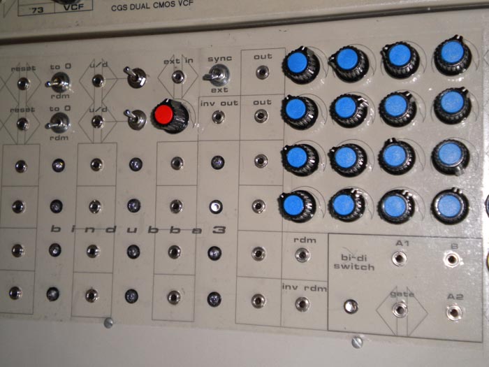
BINDUBBA 3 up/down/sideways/forward/backward SEQUENCER
This sequencer has two sets of inputs, a CV out, inverted CV out, random out, inverted random out and 16 gate outs.
If the pots/LEDs/gates are laid out in a 4x4 matrix, one set of inputs controls horizontal movement, the other vertical.
Each set of inputs has a clock input, reset and up/down. The clocks can be linked so the horizontal clock will drive the vertical section on every 16th step.
More interesting is to have two quite different clocks driving the circuit to get complex patterns forming.
An example of counting would be: 1, 2,v 7, 8,v 9, 10, 11,v 16, 13, 14,v 3, 4...The 'v' indicates a vertical clock pulse.
Then you can start messing with the up/down direction to really get a groove on!
The counters can be manually or gate controlled to count up or down. The reset inputs can reset the count back to the 1st stage or be switched to random reset.
In this case the Q3, Q4 outputs of the 4029 counters will determine the reset point, but there is no easy way of knowing what that will be, so it is essentially random.
The LEDs and current limiting/gate resistors have been left off the PCB, these are to be mounted on the panel.
It is assumed the gate jacks and LEDs will be positioned next to each other, so it is quite simple to connect these with resistors.
This method saves connecting 32 wires from the PCB to panel and reduces PCB real estate.
The random outs are derived from a resistor D/A network on the Q1-Q4 outputs of the 4029 counters.
The D/A network is split over the two counters, Q1-Q4 of U3 supplying the LSB half and Q1-Q4 of U6 supplying the MSB half.
As the two counters will be running off different clocks, and may be counting forwards or backwards, it means the voltage coming from the D/A network will be difficult, if not impossible to predict.
23/6/2010 - A prototype has been built, the design went through a few changes to get the circuit to work as desired. The modified schematic is below. The schematic only shows the subcircuits for two of the led/gate sections. The other 14 are easy enough to work out from observing the connections of these two. The gate/led circuits are powered by op-amp summers. The op-amp noninverting inputs are held low (-12V), one +12V signal from 0ne of the 4052 ICs brings the output to 0V, a 2nd +12V signal brings the output to +12V and lights up the led.
Bindubba3 full schematic tested [vers.4 1/7/2010](jpeg 500kB)
](http://www.sdiy.org/pinky/data/bindubba3.jpg)
Bindubba3 early Serge style panel design (125kB)
Bindubba3 construction notes updated 1/7/2010 (300kB)